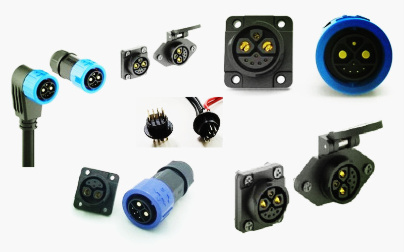
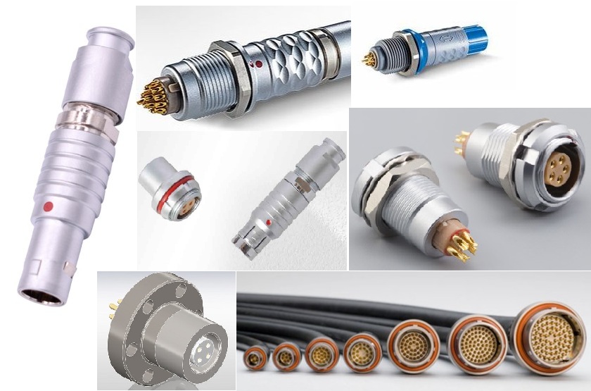
Two PCBs are never ideal planes. Each board carries its own thickness tolerance, copper distribution, warp from reflow, and variation from routing and depaneling. When a connector is chosen only from an electrical table, the layout may have no shared reference for the mating face, board edge, and mounting holes. One board sits slightly high, the other is slightly rotated, and the contact array absorbs the difference. That is manageable for a small signal connector with generous clearance. It becomes a different problem when the interface combines a dense 32-pin field with 40A power contacts, because the housing is larger, insertion force is higher, and the contact array has less room to forgive a tilted mating face. A common assembly review situation makes the risk visible. The CAD stack looks correct, the electrical check passes, and the connector is approved on paper. During first article, the connector seats with a visible gap on one side or needs unusual force to latch. The natural response is to blame the connector, but the cause is often the board pair: one PCB is warped after reflow, the connector was placed from a different datum than the mounting holes, or the housing reaches its stop before the contacts fully engage. Connector-aware design treats the mated pair as one mechanical assembly. It defines a common datum, checks connector position against mounting features, and reviews housing clearance before the layout is frozen.

 +86-15817275200